
این متن دومین مطلب آزمایشی من است که به زودی آن را حذف خواهم کرد.
زکات علم، نشر آن است. هر
وبلاگ می تواند پایگاهی برای نشر علم و دانش باشد. بهره برداری علمی از وبلاگ ها نقش بسزایی در تولید محتوای مفید فارسی در اینترنت خواهد داشت. انتشار جزوات و متون درسی، یافته های تحقیقی و مقالات علمی از جمله کاربردهای علمی قابل تصور برای ,بلاگ ها است.
همچنین
وبلاگ نویسی یکی از موثرترین شیوه های نوین اطلاع رسانی است و در جهان کم نیستند وبلاگ هایی که با رسانه های رسمی خبری رقابت می کنند. در بعد کسب و کار نیز، روز به روز بر تعداد شرکت هایی که اطلاع رسانی محصولات، خدمات و رویدادهای خود را از طریق
بلاگ انجام می دهند افزوده می شود.
این متن اولین مطلب آزمایشی من است که به زودی آن را حذف خواهم کرد.
مرد خردمند هنر پیشه را، عمر دو بایست در این روزگار، تا به یکی تجربه اندوختن، با دگری تجربه بردن به کار!
اگر همه ما تجربیات مفید خود را در اختیار دیگران قرار دهیم همه خواهند توانست با انتخاب ها و تصمیم های درست تر، استفاده بهتری از وقت و عمر خود داشته باشند.
همچنین گاهی هدف از نوشتن ترویج نظرات و دیدگاه های شخصی نویسنده یا ابراز احساسات و عواطف اوست. برخی هم انتشار نظرات خود را فرصتی برای نقد و ارزیابی آن می دانند. البته بدیهی است کسانی که دیدگاه های خود را در قالب هنر بیان می کنند، تاثیر بیشتری بر محیط پیرامون خود می گذارند.
Technological advances have ensured that Printed Circuit Boards cannot only perform complex functions they can also be produced inexpensively. This is the exact reason why PCBs are an integral part of so many devices. However, the quality of the device is directly proportional to the quality of the PCB used. PCB failure can, therefore, have debilitating consequences wherein entire systems can fail. It is therefore extremely important to stick to some quality measures in the PCB design and manufacturing process.
IPC Standards
The Institute for Printed Circuit Boards (actually, it is a name the association was formerly known as; currently it is called Association Connecting Electronics Industries, even though it has retained the IPC moniker) is a global trade association, which has set certain standards for the manufacture of PCBs as well as other electronic components. Founded in 1957, the institute releases acceptability standards for Printed Circuit Boards. The Industry Association has over 4000 members that make and design PCBs and assemblies, which include but are not limited to the following industries:
IPC standards, therefore, are industry-adopted standards for nearly every step of PCB manufacturing, beginning with design, production, and finally for electronic assembly.
There are a number of benefits that accrue from adhering to IPC standards issued by the industry body, primary among them being:
As per IPC there are several advantages of being trained and certified to use IPC standards. These include:
IPC standards come in a variety of classes. One of the commonly used one being the IPC-A-610. Some of the elements that IPC-A-610 covers includes but is not limited to:
Some of the basic principles of the IPC-A-610 classes are:
This is applicable for General Electronic Products where the major requirement is function of the completed assembly. This is therefore considered as one of the most lenient classes when it comes to allowing potential defects and therefore isn’t one that OEMs request.
This is the standard that is very often put to use for non-critical assemblies where long term reliability is a pre-requisite, although this class also allows for some degree of imperfection.
This is the highest standard, meant for the more critical PCB assemblies. A good CEM provider will therefore manufacture products to class 3 standards. This does call for a higher cost as there is extra inspection involved as well as the need to slow down surface mount machines to ensure the required placement accuracy. Conversely, it may sometimes require an allowance for higher degrees of scrap.
The advantage of using the IPC standards also stems from the fact that they have worldwide acceptance and that they have been tested across myriad industries. However if there is any conflict when it comes to acceptance of the product, as per the IPC, the following order of precedence applies:
-Procurement as agreed and documented between customer and supplier
-Master drawings
– IPC-A-610
IPC has also defined conditions that help refine processes. These conditions include:
Target Condition – This is a near perfect condition, which is the ideal to aim for, even though it may not always be achievable
Acceptable Condition – While this condition may not be ideal as there could be trade offs between design and performance, however this condition maintains reliability.
Defect Condition- This is where the product is rejected as it needs rework or repair
Process Indicator Conditions – These are conditions that aren’t known to affect either the form or function of the product but emanate from material, design or machine related factors.
Essentially then, IPC Standards help the manufacturer to clearly understand customer requirements and deliver up to expectations. As a customer you can select the IPC standard class and be rest assured that the product will live up to your requirements.
Unless your PCB is designed correctly in the first place, you are going to run into issues sooner or later.
Designing a PCB for one of today's products can be very complex, but this aspect of things is often overlooked. Instead, the focus falls upon the more "interesting" aspects of the product, like the FPGAs or MCUs. The fact remains, however, that unless the board is designed correctly in the first place, you are going to run into issues sooner or later.
The following are the main aspects of a modern PCB about which we should be particularly concerned:
1. PCB stack-up: This is the keystone of the entire PCB. It defines the number of layers within the PCB (more layers can increase the cost) and allows the engineering team to establish the characteristic impedances on the various layers. Like many things in engineering, this becomes a trade-off between fabrication processes and layer count to achieve the desired reliability, yield, and cost targets.
2. Via types: Vias enable interconnections between the layers and components. There are many different types of vias: Through, Buried, Blind, and Micro (single-layer, multi-layer, or stacked). The best designs minimize the different types of via. Close discussion with your selected PCB supplier is also important to ensure that the via types you wish to use is within their capabilities. You will also need to ensure the current carrying capacity of the different via types (you can parallel up to accommodate high current paths).
3. Design rules: These will address rules for the design itself; e.g., component placement, crosstalk budgets, layer allocation, length matching/time of flight analysis, and so on. This will also include design for manufacture (DFM) rules, which ensure the finished design can actually be manufactured; i.e., are the via aspect ratios correct?
4. Breakout strategy: Before you can begin to verify your signal and power integrity, you must first ensure you can break out and route all of the signals on high-pin-count devices. This will also affect the stack-up of the PCB -- should you use micro-via breakout (most probably yes) and how deep should these be stacked? Once you have a defined stack for the PCB, you can decide on your routing strategy -- will it be the traditional North, South, East, and West, a layer-based breakout, or a hybrid style?
5. Signal integrity: This is one of the most commonly considered aspects of designing a good PCB. Typically, an engineer will consider things such as the signal rise and fall times, track lengths and characteristic impedances, and the drive strength and slew rates of the drivers and terminations. To ensure the best performance, signal integrity (SI) simulations on the PCB will be performed pre-layout and post-layout; you will also need to consider the crosstalk budget.
6. Power integrity: High-performance devices -- especially modern FPGAs and ASICs -- can require large currents at low voltages. Ensuring both the DC and AC performance of the power distribution network is of vital importance.
Of course, the above list is by no means complete; however, it does provide a good starting point. I will consider some of these aspects in more detail in future blogs and also look at the tasks of assembling and populating the finished PCB.
برد مدار چاپی یا PCB مخفف
Printed Circuit Board
می باشد. در حقیقت برد مدار چاپی معمولا از جنس فایبرگلاس می باشد و این امکان را ایجاد می کند که بتوانیم قطعات الکترونیکی را روی آن مونتاژ کنیم و پایه های آن قطعات را به ترتیبی که در مدار شماتیک ترسیم و طراحی شده به هم متصل نماییم.
اختراع برد مدار چاپی از ابتدای قرن بیستم توسط دانشمندان مختلف آغاز شد و در نهایت در جنگ جهانی دوم در سال 1943 توسط کشور آمریکا به تولید انبوه رسید. پس از جنگ، در سال 1948، ایالات متحده آمریکا این اختراع را برای استفاده تجاری منتشر کرد و از آن پس شاهد استفاده برد مدارچاپی در هر دستگاه الکترونیکی از ساده ترین اسباب بازی ها تا پیچیده ترین دستگاه های مخابراتی، نظامی و فضایی هستیم.
در هر دستگاه الکترونیکی برد مدار چاپی از اهمیت بسزایی برخوردار است. به عنوان مثال به موارد زیر توجه کنید:
1. تمامی قطعات و اتصالات برد الکترونیکی بر روی برد مدار چاپی است، لذا حتما باید تعداد لایه و جنس برد مدار چاپی با دقت انتخاب شود.
2. به دلیل اینکه تمامی مدار الکترونیکی در برد مدارچاپی پیاده سازی شده است، از این رو نحوه پیاده سازی بسیار مهم می گردد. به عبارت دیگر باید توجه ویژه به مسیر جریان الکتریکی، محل قرار گرفتن خازن های نویز گیر، نحوه اتصال برد به بدنه دستگاه، مسایل مربوط به فرکانس بالا، امپدانس خطوطی که سیگنال فرکانس بالا دارد، مسایل مربوط به برد های چند لایه، مسایل مربوط به چیدمان قطعات از لحاظ فشردگی و سهولت مونتاژ و نکات بسیار زیاد دیگر که به تفصیل توضیح داده خواهد شد.
با توجه به نکات فوق که شامل چند مثال ساده از مسائل برد مدارچاپی بود، مشخص می شود برد مدارچاپی می تواند نقش بسزایی در موفقیت و عدم موفقیت یک پروژه داشته باشد. لذا در ادامه به نکات کاربردی که حاصل سالها تجربه و مطالعه است اشاره خواهم کرد.
دانش کافی نسبت به روشها و مراحل ساخت برد مدار چاپی داشته باشید.
به نظر میرسد تعداد زیادی از مهندسین طراح، آشنایی کاملی با روشها و مراحل مختلف تولید بردهای مدار چاپی ندارند. فقدان این دانش کاربردی می تواند اغلب باعث شود که طراحان تازه کار طرح هایی که پیچیده تر از حد مورد نیاز است پیاده سازی نمایند. در نگاه اول ممکن است طرح آنها پیچیده و پیشرفته جلوه کند اما بی شک مشکلات فراوانی به همراه خواهد داشت. به عنوان مثال، یک اشتباه رایج تازه کاران این است که ابعاد طرح را بسیار دقیق تعیین کرده و از ترکهای با فواصل بسیار نزدیک و با خمهای نود درجه استفاده میکنند. باید توجه کرد که علاوه بر عدم قابلیت اطمینان کافی در این نوع طراحی، ممکن است سازندههای کمی قادر به تولید چنین بردهای دقیقی باشند.
![]()
تولیدکنندگان توانا نیز احتمالا قیمت اقتصادی و قابل رقابت ارایه نخواهند کرد. آیا طراحی واقعا باید پیچیده باشد؟ آیا ترکها نمیتوانند درفاصله مناسب تری از هم قرار بگیرند تا هم هزینه های ساخت را کاهش داده و هم قابلیت اطمینان را بهبود بخشد؟
از اشتباهات دیگر طراحان تازه کار میتوان به ویاهای بسیار کوچک و یا استفاده غیر ضروری از ویای کور و مدفون اشاره کرد. وجود چنین قابلیتهایی مسلما کاربردی است اما موثر بودنشان به شرایط خاصی بستگی دارد. فقط به این دلیل که چنین امکاناتی در فاز طراحی در اختیار هستند، به این معنا نیست که حتما باید استفاده شوند!
در مورد اندازه یک ویا، انتخاب نسبت 6:1 در حد زیادی تضمین میکند که برد شما توسط اکثر تولیدکنندگان قابل ساخت است. در بسیاری از طرح ها با کمی دقت و نقشه ریزی میتوان مناسب بودن هزینه تولید و همچنین قابلیت ساخت را برآورده کرد. در نظر داشته باشید تنها وجود یک ویای بد میتواند کل برد را بلا استفاده کند! حال وجود 20000 ویا میتواند شانس خرابی را 20000 برابر کند. سایر موارد پیچیده نیز به این احتمال می افزاید!
طراحی بخش تغذیه، مهمترین بخش طراحی برد مدار چاپی می باشد. وظیفه بخش تغذیه تامین ولتاژ و جریان برد مدارچاپی می باشد . لذا طراحی این بخش باید با حساسیت زیاد انجام گردد. برای طراحی این بخش استراتژی های مختلفی وجود دارد.
اولین و مهم ترین اصل برای این قسمت، حداقل بودن امپدانس خط انتقال تغذیه است. لذا برای این منظور معمولا قطر ترک (trace) باید به اندازه کافی پهن انتخاب شود. سوالی که مطرح می شود این است که چقدر باید پهن باشد؟
پاسخ این سوال بستگی دارد به جریان عبوری، هر چقدر جریان عبوری بیشتر باشد، باید قطر پهن تر باشد. اما برای جاهایی که نمی توان قطر ترک را پهن کرد چه باید کرد؟ معمولا در این شرایط سعی می کنند تعداد لایه ها را افزایش دهند مثلا دو، چهار و یا حتی از لایه های بیشتر استفاده می کنند؛ که این مسئله باعث افزایش هزینه برای پروژه است.
راه حل دیگر که تعداد لایه ها لازم نیست افزایش یابد، برداشتن چاپ سبز ( solder mask ) از روی ترک اصلی جریان بالا است، سپس با افزودن قلع بر روی ترک قطر ترک افزایش خواهد یافت. البته این روش زیاد توصیه نمی شود چون ممکن است مونتاژ کار بر روی بردی زیاد لحیم بزند و جای دیگر کلا فراموش کند!
از ابزار Autorouter استفاده کنید، اما اعتماد نه!
اکثر برنامه های حرفه ای طراحی برد ابزاری به نام مسیریابی خودکار دارند. ولی یک طراح حرفه ای تمام زحمت طراحی را به عهده این ابزار نمیگذارد! آگاهی به روشهای مسیر کشی دستی از مومات کار است. مسیریاب خودکار، ابزاری قابل اعتماد است به شرطی که یک سری نکات در استفاده از آن رعایت شود.
پارامترهای مربوط به این ابزار بایستی در هر مداری جداگانه و متناسب نیازمندی های آن طرح و به طور هوشمند و دقیق تنظیم شوند. حتی ممکن است هر بخشی از مدار نیازمندی های خاص خود را داشته باشد. اگر از یک طراح حرفه ای بپرسید بهترین ابزار مسیریاب کدام است پاسخ خواهد داد مغز شما! و چه پاسخ شایسته ای!
این ابزارها از الگوریتم های خاصی مانند الگوریتم مسیر بازگشتی(backtracking) برای مسیربابی استفاده میکنند، مشابه آنچه در حل پازلها یا مارپیچها استفاده میشود. اما در یک طرح مدار چاپی که قطعات ابتدا جانمایی شده و همچنین قیود خاصی مطرح نیستند، راه حل بهینه ای نخواهد بود. حتی اگر این قیود توسط طراح در ابزار تنظیم شوند نیز باز طرح نهایی نیاز به بازبینی موشکافانه توسط طراح خواهد داشت.

از مشکلات استفاده از این ابزار میتوان به ضخامت خطوط اشاره کرد. فقط طراح است که میداند از هر مسیری چه جریانی عبور میکند! Aoutorouter همه مسیرها را با عرض یکسان در نظر خواهد گرفت. حتی اگر تنظیمات مربوطه را نیز با دقت انجام داده باشید باز هم قسمتی خواهد بود که به بازبینی طراح نیاز داشته باشد.
طراحان حرفه ای میگویند نصف(یا حی بیشتر) زمان لازم برای طراحی میبایست صرف جانمایی بهینه قطعات شود. زیرا:
ساده سازی مسیریابی و حداقل استفاده از جامپرها
نزدیکی قطعات و منظم شدن طرح، به خصوص بخش بندی عملکردی مدار. یعنی مثلا بخش تغذیه کنار هم یا واحد پردازنده کنار هم یا . . هر چه مسیرها کوتاه تر باشند بهتر هستند.
رفع نگرانی ها در مورد زمان سیگنال (Signal Timing)
با کمی خلاقیت میتوان بهترین استفاده را زا این ابزار برد. مثلا قسمت های مهم را به روش دستی مسیریابی کرد و سپس با قفل کردن مسیرهای طراحی شده، قسمت های باقیمانده را توسط ابزار خودکار کامل کرد!.
طراحی شماتیک، صرفه جویی در خطایابی
گاهی اوقات مهندسان تازه کار از طراحی شماتیک در طرح های ساده امتناع میکنند و آن را هدردادن زمان میدانند. به خصوص اگر قبلا یک یا دو طراحی مشابه انجام داده باشند. برای اولین بار ممکن است کشیدن شماتیک دلهره آور به نظر برسد. حتی طراحان با تجربه تر هم گاهی از این مرحله صرف نظر میکنند!
مهندسان گرامی! در مقابل این وسوسه مقاومت کنید!! داشتن یک طرح شماتیک کامل از مدار و استفاده از آن به عنوان مرجع صحیح ارتباطات بین اجزا بسیار مفید خواهد بود. وجود تمام قطعات در یک سند و مشخص بودن ارتباطات تک تک اتصالات در مرحله طراحی pcb کمک بزرگی خواهد بود. با اطمینان این حرف را میگویم. اعتماد کنید!
اول اینکه: طرح شماتیک یک نمایش بصری از مدار است و اطلاعات را در چند سطح به هم مرتبط میسازد. کل طرح میتواند به چند بخش از نظر عملکردی تقسیم شود و قطعات مرتبط کنار هم قرار بگیرند(بدون توجه به اینکه در طرح واقعی کجا جانمایی میشوند)
دوم اینکه: شماتیک کمک میکند از کامل بودن یا نبودن طرح مطمعن شویم. وقتی هر پایه از هر قطعه ای در مدار شماتیک مشخص بوده و اتصال به پایه ی هدف نیز تعیین شده باشد پیدا کردن پایه های متصل نشده کار آسانی خواهد بود. به عبارت دیگر صرف نظر از اینکه قواعد معمول طراحی در نظر گرفته شده باشند یا نه، با داشتن طرح شماتیک، پیدا کردن خطاهای اتصال به صورت بصری فراهم خواهد بود و آسان.
وقتی طرح شماتیک کامل و اتصالات مشخص شده باشند، در محیط طراحی pcb خطوطی به عنوان راهنمای اتصالات نمایش داده شده و شما را از فکر کردن به اینکه چه پایه ای به کجا باید وصل شود رهانیده و خطایابی نیز بسیار سریع تر و آسانتر خواهد بود.
به قوانین طراحی(DRC) توجه کنید
در اکثر برنامه های طراحی pcb، ابزاری تحت عنوان کنترل کننده قوانین طراحی(DRC) و یاconstraint managers” وجود دارد. نکاتی که در بخش تنظیمات Aoutorouterمطرح شد بیشتر به عملکرد مدار مربوط بود اما در بخش DRC با اعمال تنظیماتی میتوان از ابتدا محدودیتهای مربوط به فرآیند تولید(مانند حداقل عرض مسیرها و یا حداقل اندازه سوراخ ها و یا .) را در نرم افزار اعمال کرد تا به این ترتیب در حین طراحی مدار، این محدودیت ها پیوسته کنترل شده و در صورت عدم رعایت، هشدار داده شود. هرچقدر در شناخت محدودیت ها آگاهتر باشید و به طور دقیق در تنظیمات مربوطه اعمال کنید، به همان میزان زمان طراحی و قابلیت اطمینان طرح را بالا برده اید.
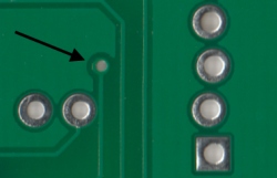
جلوگیری از ایجاد ضایعات
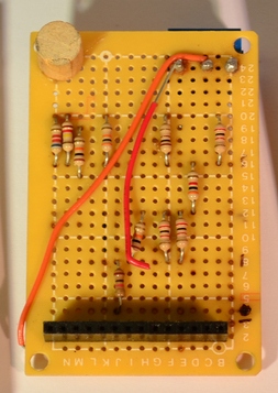
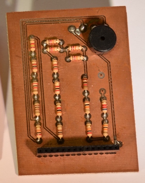
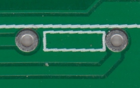
طراحی مناسب مسیرها، میتواند به پروسه ساخت کمک کرده و از ایجاد ضایعات و تراشه ها جلوگیری نماید(شکل1). برای فهم بهتر این نکته، به فرآیند حذف لایه های اضافی مس در تولید برد توجه کنید. این فرآیند شیمیایی با پوشش دهی به قسمتهایی که باید باقی بمانند و سپس گذاشتن برد در حمام اسیدی اتفاق میافتد. حال اگر با توجه به نوع طراحی، مثلا قسمتی بسیار طولانی و با عرض کم وجود داشته باشد، به طور کامل از برد جدا شده و این لایه مسی سرگردان در حمام قلع ممکن است به بردهای دیگر و یا قسمتهای دیگری از مدار چسبیده و باعث بروز اتصال های ناخواسته در جاهای دیگر شود!

برای جلوگیری از بروز مشکلات اینچنینی، نهایت دقت و توجه را به کار ببرید و از ایجاد فضاهای باریک و طولانی بین مسیرها در طرح اجتناب کنید(شکل 2 و 3). این فواصل را از حداقل مقدار ممکن اعلام شده از طرف تولیدکنندگان برد ، بالاتر در نظر بگیرید. عموم سازندگان مقدار فاصله بین خطوط را 0.16mm اعلام مینمایند.
مشخصات هندسی طرح و گردش جریان در مدار
شارش الکترونها در مدار و ایجاد جریان الکتریکی همانند عبور رودخانه در مسیر خود، ممکن است به پیج و خم ها و تنگناهایی برخورد کند. وجود این تنگناها منتهی به ایجاد یک فیوز خودکار در مدار میشود! مثلا تنظیم یک مسیر به شکل V با زاویه خمش زیاد و عرض باریک آن باعث میشود در نقطه خاصی از جریان، مقاومت مسیر تحمل نداشته و به دمای ذوب رسیده و باعث قطع مدار شود! نکته اینجاست که طراحان عزیز ناخودآگاه از این فیوزها در طرح خود استفاده میکنند. یک خمش نود درجه اگر با دو خمش 45 درجه جایگزین شود بسیار بهینه تر خواهد بود. زوایای خمش زیاد مانند شکل V باعث کاهش سرعت انتشار سیگنال و حالت سوئیچبک میشود و حتی ممکن است ناخواسته باعث ایجاد یک اتوفیوز گردد.
تولیدکننده مناسب خود را بشناسید
پس از اشاره به نکات مربوط به فاز طراحی، ذکر این نکته خالی از لطف نیست که شناخت تولیدکننده مورد نظر و آگاهی از قوانین و توانمندیهای سازنده میتواند در زمان و هزینه شما صرفه جویی ایجاد کند. حداقل فاصله بین مسیرها، قطر سوراخ ها، تعداد لایه ها، جنس فیبر و گرید مورد استفاده و . همه از نکات مهمی هستند که قبل از شروع طراحی باید در نظر گرفته شوند و بنابر نیاز، تولید کننده مناسب انتخاب شود. جنس و نوع متریال استفاد شده در میزان عمر، قابلیت اطمینان، مقاموت حرارتی و عملکرد مدار بسیار اثرگذار است. بعضی از تولیدکنندهها در تولیدت نمونه از جنس FR4 استفاده میکنند ولی در تولیدات با حجم بالا FR2 را جایگزین میکنند.
گروه طراجی برد مدار چاپی با بیش از 20 سال تجربه در طراحی، تولید و ساخت انواع برد مدار چاپی PCB و همکاری با شرکت های صنعتی، می تواند به شما در به هدف رساندن پروژه های الکترونیکی کمک شایانی نماید.
پدیده نویز، یکی از مهمترین مباحث در الکترونیک می باشد. طراح خوب برد مدارچاپی باید درک درست و توجه خاصی در هنگام طراحی به این موضوع داشته باشد. نویز در مدارات الکترونیکی یا منشا خارجی دارد یا داخل برد تولید می شود.
برای مقابله و کاهش تاثیر نویز خارجی که در شرایط خاص به آن نویز سفید هم می گویند راه حل های مختلفی وجود دارد. که یکی از پرکاربرد ترین روش ها، شیلد کردن برد و نصب قاب فی بر روی برد و اتصال بدنه به ارت می باشد.
برای کنترل و کاهش نویز در داخل برد، باید به چیدمان قطعات و قرار دادن خازن نویز گیر و حتی شیلد کردن محل تولید نویز توجه خاصی شود.
#نویز
به قوانین طراحی(DRC) توجه کنید
در اکثر برنامه های طراحی pcb، ابزاری تحت عنوان کنترل کننده قوانین طراحی(DRC) و یاconstraint managers” وجود دارد. نکاتی که در بخش تنظیمات Aoutorouterمطرح شد بیشتر به عملکرد مدار مربوط بود اما در بخش DRC با اعمال تنظیماتی میتوان از ابتدا محدودیتهای مربوط به فرآیند تولید(مانند حداقل عرض مسیرها و یا حداقل اندازه سوراخ ها و یا .) را در نرم افزار اعمال کرد تا به این ترتیب در حین طراحی مدار، این محدودیت ها پیوسته کنترل شده و در صورت عدم رعایت، هشدار داده شود. هرچقدر در شناخت محدودیت ها آگاهتر باشید و به طور دقیق در تنظیمات مربوطه اعمال کنید، به همان میزان زمان طراحی و قابلیت اطمینان طرح را بالا برده اید.
جلوگیری از ایجاد ضایعات
طراحی مناسب مسیرها، میتواند به پروسه ساخت کمک کرده و از ایجاد ضایعات و تراشه ها جلوگیری نماید(شکل1). برای فهم بهتر این نکته، به فرآیند حذف لایه های اضافی مس در تولید برد توجه کنید. این فرآیند شیمیایی با پوشش دهی به قسمتهایی که باید باقی بمانند و سپس گذاشتن برد در حمام اسیدی اتفاق میافتد. حال اگر با توجه به نوع طراحی، مثلا قسمتی بسیار طولانی و با عرض کم وجود داشته باشد، به طور کامل از برد جدا شده و این لایه مسی سرگردان در حمام قلع ممکن است به بردهای دیگر و یا قسمتهای دیگری از مدار چسبیده و باعث بروز اتصال های ناخواسته در جاهای دیگر شود!
برای جلوگیری از بروز مشکلات اینچنینی، نهایت دقت و توجه را به کار ببرید و از ایجاد فضاهای باریک و طولانی بین مسیرها در طرح اجتناب کنید(شکل 2 و 3). این فواصل را از حداقل مقدار ممکن اعلام شده از طرف تولیدکنندگان برد ، بالاتر در نظر بگیرید. عموم سازندگان مقدار فاصله بین خطوط را 0.16mm اعلام مینمایند.
مشخصات هندسی طرح و گردش جریان در مدار
شارش الکترونها در مدار و ایجاد جریان الکتریکی همانند عبور رودخانه در مسیر خود، ممکن است به پیج و خم ها و تنگناهایی برخورد کند. وجود این تنگناها منتهی به ایجاد یک فیوز خودکار در مدار میشود! مثلا تنظیم یک مسیر به شکل V با زاویه خمش زیاد و عرض باریک آن باعث میشود در نقطه خاصی از جریان، مقاومت مسیر تحمل نداشته و به دمای ذوب رسیده و باعث قطع مدار شود! نکته اینجاست که طراحان عزیز ناخودآگاه از این فیوزها در طرح خود استفاده میکنند. یک خمش نود درجه اگر با دو خمش 45 درجه جایگزین شود بسیار بهینه تر خواهد بود. زوایای خمش زیاد مانند شکل V باعث کاهش سرعت انتشار سیگنال و حالت سوئیچبک میشود و حتی ممکن است ناخواسته باعث ایجاد یک اتوفیوز گردد.
از ابزار Autorouter استفاده کنید، اما اعتماد نه!
اکثر برنامه های حرفه ای طراحی برد ابزاری به نام مسیریابی خودکار دارند. ولی یک طراح حرفه ای تمام زحمت طراحی را به عهده این ابزار نمیگذارد! آگاهی به روشهای مسیر کشی دستی از مومات کار است. مسیریاب خودکار، ابزاری قابل اعتماد است به شرطی که یک سری نکات در استفاده از آن رعایت شود.
پارامترهای مربوط به این ابزار بایستی در هر مداری جداگانه و متناسب نیازمندی های آن طرح و به طور هوشمند و دقیق تنظیم شوند. حتی ممکن است هر بخشی از مدار نیازمندی های خاص خود را داشته باشد. اگر از یک طراح حرفه ای بپرسید بهترین ابزار مسیریاب کدام است پاسخ خواهد داد مغز شما! و چه پاسخ شایسته ای!
این ابزارها از الگوریتم های خاصی مانند الگوریتم مسیر بازگشتی(backtracking) برای مسیربابی استفاده میکنند، مشابه آنچه در حل پازلها یا مارپیچها استفاده میشود. اما در یک طرح مدار چاپی که قطعات ابتدا جانمایی شده و همچنین قیود خاصی مطرح نیستند، راه حل بهینه ای نخواهد بود. حتی اگر این قیود توسط طراح در ابزار تنظیم شوند نیز باز طرح نهایی نیاز به بازبینی موشکافانه توسط طراح خواهد داشت.
از مشکلات استفاده از این ابزار میتوان به ضخامت خطوط اشاره کرد. فقط طراح است که میداند از هر مسیری چه جریانی عبور میکند! Aoutorouter همه مسیرها را با عرض یکسان در نظر خواهد گرفت. حتی اگر تنظیمات مربوطه را نیز با دقت انجام داده باشید باز هم قسمتی خواهد بود که به بازبینی طراح نیاز داشته باشد.
طراحان حرفه ای میگویند نصف(یا حی بیشتر) زمان لازم برای طراحی میبایست صرف جانمایی بهینه قطعات شود. زیرا:
ساده سازی مسیریابی و حداقل استفاده از جامپرها
نزدیکی قطعات و منظم شدن طرح، به خصوص بخش بندی عملکردی مدار. یعنی مثلا بخش تغذیه کنار هم یا واحد پردازنده کنار هم یا . . هر چه مسیرها کوتاه تر باشند بهتر هستند.
رفع نگرانی ها در مورد زمان سیگنال (Signal Timing)
با کمی خلاقیت میتوان بهترین استفاده را زا این ابزار برد. مثلا قسمت های مهم را به روش دستی مسیریابی کرد و سپس با قفل کردن مسیرهای طراحی شده، قسمت های باقیمانده را توسط ابزار خودکار کامل کرد!.
طراحی شماتیک، صرفه جویی در خطایابی
گاهی اوقات مهندسان تازه کار از طراحی شماتیک در طرح های ساده امتناع میکنند و آن را هدردادن زمان میدانند. به خصوص اگر قبلا یک یا دو طراحی مشابه انجام داده باشند. برای اولین بار ممکن است کشیدن شماتیک دلهره آور به نظر برسد. حتی طراحان با تجربه تر هم گاهی از این مرحله صرف نظر میکنند!
مهندسان گرامی! در مقابل این وسوسه مقاومت کنید!! داشتن یک طرح شماتیک کامل از مدار و استفاده از آن به عنوان مرجع صحیح ارتباطات بین اجزا بسیار مفید خواهد بود. وجود تمام قطعات در یک سند و مشخص بودن ارتباطات تک تک اتصالات در مرحله طراحی pcb کمک بزرگی خواهد بود. با اطمینان این حرف را میگویم. اعتماد کنید!
اول اینکه: طرح شماتیک یک نمایش بصری از مدار است و اطلاعات را در چند سطح به هم مرتبط میسازد. کل طرح میتواند به چند بخش از نظر عملکردی تقسیم شود و قطعات مرتبط کنار هم قرار بگیرند(بدون توجه به اینکه در طرح واقعی کجا جانمایی میشوند)
دوم اینکه: شماتیک کمک میکند از کامل بودن یا نبودن طرح مطمعن شویم. وقتی هر پایه از هر قطعه ای در مدار شماتیک مشخص بوده و اتصال به پایه ی هدف نیز تعیین شده باشد پیدا کردن پایه های متصل نشده کار آسانی خواهد بود. به عبارت دیگر صرف نظر از اینکه قواعد معمول طراحی در نظر گرفته شده باشند یا نه، با داشتن طرح شماتیک، پیدا کردن خطاهای اتصال به صورت بصری فراهم خواهد بود و آسان.
وقتی طرح شماتیک کامل و اتصالات مشخص شده باشند، در محیط طراحی pcb خطوطی به عنوان راهنمای اتصالات نمایش داده شده و شما را از فکر کردن به اینکه چه پایه ای به کجا باید وصل شود رهانیده و خطایابی نیز بسیار سریع تر و آسانتر خواهد بود.
مدارات تقویت کننده به واسطه تقویت سیگنال کوچک اگر درست طراحی نشود کار نخواهند کرد!!
برای طراحی این نوع مدارات باید به دو بخش تغذیه و ورودی مدار توجه ویژه داشت.
۱. این نوع مدارات معمولا به خاطر تقویت سیگنال، جریان بالا مصرف می کنند لذا باید خازن های الکترولیت مناسب با توجه به مصرف جریان نزدیک پایه تغذیه قرار داد. در ضمن سعی شود مدار، جایی قرار گیرد که فاصله آن تا منبع تغذیه کم باشد. اگر فاصله به ناچار زیاد شد، حتما قطر ترک پهن انتخاب شود تا افت ولتاژ کمتر باشد. در ضمن معمولا برای کاهش اثر این نوع مدارات بر باقی مدارات -از جهت نویز تغذیه- از فیلتر RC یا رگولاتو استفاده می شود.
۲. جهت کاهش اثر نویز بر روی سیگنال ورودی با توجه به کوچک بودن سیگنال تا آنجایی که امکان دارد فاصله مدار طبقه قبل تا ورودی این مدار کم باید باشد.
#تقویت_کننده
نکات مهمی که باید در طراحی بردمدارچاپی (PCB) رعایت کنید عبارتند از:
فوت پرینت (Footprint) کلیه قطعات را چک کنید و بررسی کنید که از لحاظ ابعادی کاملا با دیتاشیت قطعه مطابقت داشته باشد. البته اگر قطعه موجود باشد پرینت یک به یک از فوت پرینت قطعه بگیرید و با قطعه چک کنید.
پین های کلیه قطعات در شماتیک را با دیتاشیت چک کنید و مطمئن شوید که شماره پایه پین های شماتیک با شماره پین های فوت پرینتی که انتخاب کرده اید مطابقت دارد.
از اتصالات مدار شماتیک (مثلا جدا نبودن نت ها Float) اطمینان حاصل کنید.
قبل از اینکه چیدمان فیبر را انجام دهید ابعاد دقیق برد را مشخص کنید و کادر مربوطه را در لایه مکانیک بکشید.
بعد از مشخص کردن خط برش اطراف برد، اولین کار چیدمان قطعات بر روی برد است که باید فضای برد را به قسمتهای پاوری، سیگنالی، فرکانس بالا (High Frequency)، فرکانس پایین (Low Frequency)، ورودی، خروجی و … با توجه به محل ورودی و خروجی و جاهای ثابت تقسیم بندی کنید.
مهمترین قسمت طراحی یک برد مدار چاپی حرفه ای، چیدمان درست می باشد. اگر در چیدمان درست قطعات دقت کافی را داشته باشید ترکینگ (اتصال پایه به هم) مدار زمان زیادی طول نمی کشد.
اگر قصد دارید فیبر مولتی لایر طراحی کنید ابتدا باید تعداد لایه ها را مشخص کنید و در مرحله بعد باید تفکیک لایه ها را مشخص کنید و تعیین کنید که کدام لایه را به زمین و کدام لایه را به تغذیه اختصاص می دهید. معمولا لایه ای که قرار است سیگنال فرکانس بالا داشته باشد را زمین انتخاب می کنند.
ولتاژهای مدار را مشخص کنید و با توجه به ولتاژ مورد استفاده ایزولاسیون لازم را تعریف کنید.
جریانهای مدار را مشخص کنید و با توجه به جریان مورد استفاده ضخامت Track لازم را تعریف کنید.
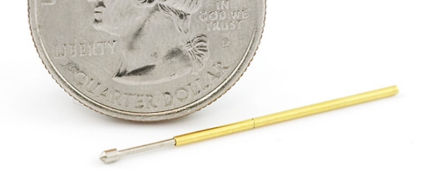
One of the key concepts in electronics is the printed circuit board or PCB. It's so fundamental that people often forget to explain what a PCB is. This tutorial will breakdown what makes up a PCB and some of the common terms used in the PCB world.
Over the next few pages, we'll discuss the composition of a printed circuit board, cover some terminology, a look at methods of assembly, and discuss briefly the design process behind creating a new PCB.
Printed circuit board is the most common name but may also be called "printed wiring boards" or "printed wiring cards". Before the advent of the PCB circuits were constructed through a laborious process of point-to-point wiring. This led to frequent failures at wire junctions and short circuits when wire insulation began to age and crack.
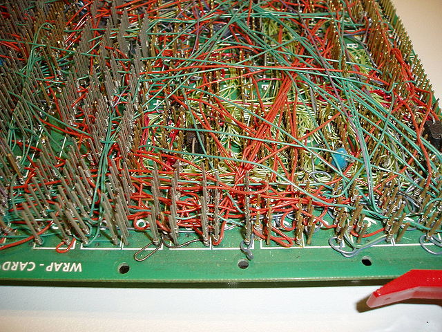
A significant advance was the development of wire wrapping, where a small gauge wire is literally wrapped around a post at each connection point, creating a gas-tight connection that is highly durable and easily changeable.
As electronics moved from vacuum tubes and relays to silicon and integrated circuits, the size and cost of electronic components began to decrease. Electronics became more prevalent in consumer goods, and the pressure to reduce the size and manufacturing costs of electronic products drove manufacturers to look for better solutions. Thus was born the PCB.
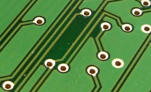
PCB is an acronym for the printed circuit board. It is a board that has lines and pads that connect various points together. In the picture above, there are traces that electrically connect the various connectors and components to each other. A PCB allows signals and power to be routed between physical devices. Solder is the metal that makes the electrical connections between the surface of the PCB and the electronic components. Being metal, the solder also serves as a strong mechanical adhesive.
A PCB is sort of like a layer cake or lasagna- there are alternating layers of
Continue . different materials that are laminated together with heat and adhesive such that a result is a single object.
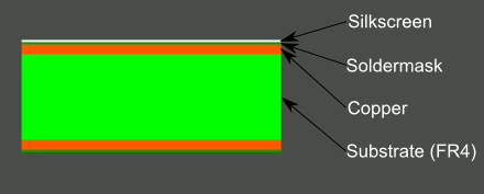
Let's start in the middle and work our way out.
The base material, or substrate, is usually fiberglass. Historically, the most common designator for this fiberglass is "FR4". This solid core gives the PCB its rigidity and thickness. There are also flexible PCBs built on flexible high-temperature plastic (Kapton or the equivalent).
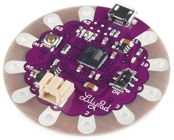
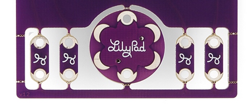
You will find much different thickness PCBs; the most common thickness for SparkFun products is 1.6mm (0.063"). Some of our products- LilyPad boards and Arduino Pro Micro boards- use a 0.8mm thick board.
Cheaper PCBs and perf boards (shown above) will be made with other materials such as epoxies or phenolics which lack the durability of FR4 but are much less expensive. You will know you are working with this type of PCB when you solder to it - they have a very distinctive bad smell. These types of substrates are also typically found in low-end consumer electronics. Phenolics have a low thermal decomposition temperature which causes them to delaminate, smoke and char when the soldering iron is held too long on the board.
The next layer is a thin copper foil, which is laminated to the board with heat and adhesive. On common, double-sided PCBs, copper is applied to both sides of the substrate. In lower cost electronic gadgets the PCB may have copper on only one side. When we refer to a double-sided or 2-layer board we are referring to the number of copper layers (2) in our lasagna. This can be as few as 1 layer or as many as 16 layers or more.
The copper thickness can vary and is specified by weight, in ounces per square foot. The vast majority of PCBs have 1 ounce of copper per square foot but some PCBs that handle very high power may use 2 or 3-ounce copper. Each ounce per square translates to about 35 micrometers or 1.4 thousandths of an inch of thickness of copper.
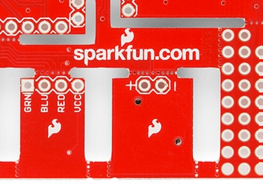
The layer on top of the copper foil is called the solder mask layer. This layer gives the PCB its green (or, at SparkFun, red) color. It is overlaid onto the copper layer to insulate the copper traces from accidental contact with other metal, solder, or conductive bits. This layer helps the user to solder to the correct places and prevent solder jumpers.
In the example below, the green solder mask is applied to the majority of the PCB, covering up the small traces but leaving the silver rings and SMD pads exposed so they can be soldered to.
Soldermask is most commonly green in color but nearly any color is possible. We use red for almost all the SparkFun boards, white for the IOIO board, and purple for the LilyPad boards.
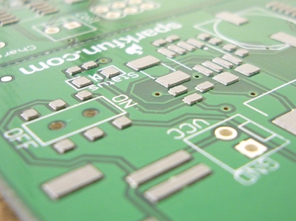
The white silkscreen layer is applied on top of the soldermask layer. The silkscreen adds letters, numbers, and symbols to the PCB that allow for easier assembly and indicators for humans to better understand the board. We often use silkscreen labels to indicate the function of each pin or LED.
The silkscreen is most commonly white but any ink color can be used. Black, gray, red, and even yellow silkscreen colors are widely available; it is, however, uncommon to see more than one color on a single board.
Now that you've got an idea of what a PCB structure is, let's define some terms that you may hear when dealing with PCBs:
ReplaceMeOpen
ReplaceMeClose
ReplaceMeOpen
ReplaceMeClose
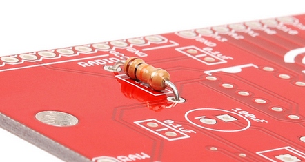
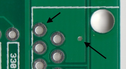
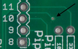
-> A small trace connecting the Reset pad to elsewhere on the board. A larger, thicker trace connects to the 5V power pin. <-
How do you go about designing your own PCB? The ins and outs of PCB design are way too in depth to get into here, but if you really want to get started, here are some pointers:
Finally, a few words on the utility of designing your own circuit boards. If you plan on making more than one or two of a given project, the payback on designing a board is pretty good- point-to-point wiring circuits on a protoboard is a hassle, and they tend to be less robust than purpose-designed boards. It also allows you to sell your design if it turns out to be popular.
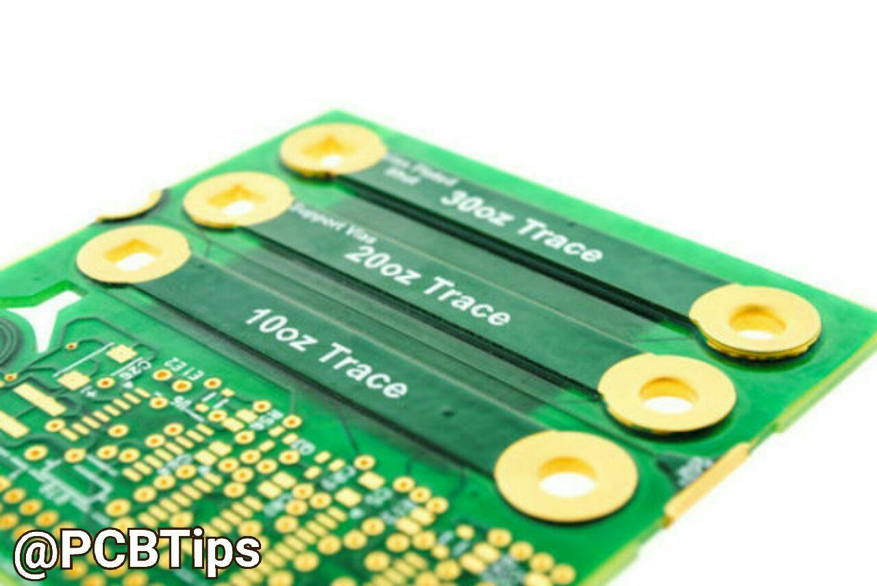 برای بیان قطر مس برد PCB از واحد oz یا اونس استفاده می کنند.
اما چرا از واحد وزن برای بیان قطر استفاده می کنند!
در تولید برد خام PCB، اهمیت به وزن مس مصرفی است نه به قطر مس!
این وزن با oz یا اونس بیان می شود و معمولا برد های خام به صورت یک اونس یا دو انس یا حتی 6 اونس تولید می شود.
وقتی مسی به وزن یک اونس در ابعاد یک فوت مربع پرس می کنند قطر آن به واحد متر 0.0347 میلی متر یا حدودا 0.035 میلی متر می شود که معادل یک oz است!
1oz = 0.0347mm or 0.035mm
یا 35 میکرون
2oz = 0.0694mm or 0.007mm
یا 70 میکرون
6oz = 0.2082mm or 0.21mm
یا 210 میکرون
برای جریان های بسیار بالا از قطر های 10oz، 15oz یا حتی 30oz استفاده می کنند.
اگر در سفارش برد PCB قطری بیان نشود به صورت پیش فرض 1oz یا 35 میکرون چاپ خواهد شد.
با خدمات #مشاوره و #طراحی_برد_مدارچاپی در خدمت شما خوبان هستم.
WhatApp: 09305667903
Designing
#PCB of
#Analog to
#Digital
#board could be a challenging project for several advanced
#PCB_designers. I designed PCB of this analog
#video to serial
#270MHz (
#SDI) for
#broadcasting proposes.
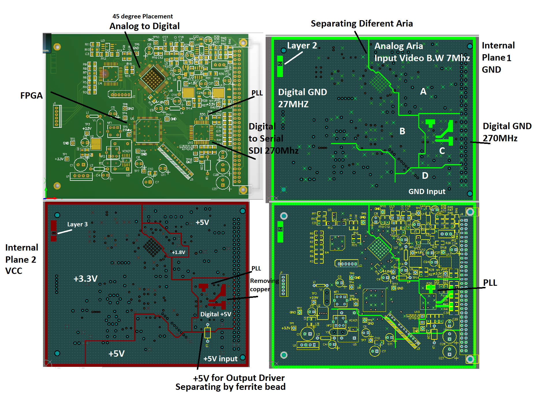
The first challenge of this kind of project is the
#routing of
#GND. The layers of PCB should be, minimum,
#four_layers, and the layer under the placement side is
#ground (GND). In the internal plane, the ground usually is separated into different sides of analog and digital. In my design, I divided the ground into three main parts A, B, and C. At first is the analog area, A, connected to the main ground from the front side of board. The second is digital ground, B, and the signal is mainly
#27Mhz and connected to the main ground from the backside. The third side is under a 270MHz parts.
As a result, in this kind of project, the ground should be separated from each other and connecting them in far point.
I will say more
#tips from this project.
@PCBandTIPs
www.pcbdesign.ir
www.pcbtips.com
#PCBTIPs
I am ready to do your
#PCB_project soon and professionally!
My WhatsApp: +1 (780) 437 1608
Cell phone: +1 (780) 437 1608
Telegram: https://t.com/PCBandTIPs
Ali Padasha

معمولا در طراحی #PCB
#مدارات
#مخابراتی، با مدار #PLL مواجه می شویم. حلقه قفل فاز (Phase-Locked Loop) یا به اختصار PLL یک
#سیستم
#کنترلی است. در واقع، حلقه قفل فاز میتواند یک سیگنال خروجی را تولید کند که
#فاز آن به فاز
#سیگنال ورودی وابسته است.
برای
#طراحی این نوع مدارات معمولا توصیه می شود در لایه وسط و لایه زیر قطعات مس حذف شود، اما چرا باید این لایه حذف شود؟
معمولا به دو دلیل این کار انجام می شود.
اول- اجتناب از خازن ایجاد شده بین لایه ها با قطعات PLL
دوم- جلوگیری از تاثیر
#میدان_الکترو_مغناطیسی و
#الکتریکی ایجاد شده بر اثر عبور جریان از مس زیر قطعات PLL و ایجاد اختلال در مدار PLL است.
اگرچه در اکثر موارد لازم به حذف مس زیر PLL است، اما قبل از این کار حتما به موارد ذکر شده مربوط به طراحی PCB در Application Note توجه کافی شود.
@PCBTIPs
www.pcbdesign.ir
www.pcbtips.com
با خدمات
#طراحی
#برد
#مدارچاپی در خدمت شما خوبان هستم.
09305667903
#نکات_طراحی_PCB
برای طراحی ترک برای جریان بالا کافی است عرض مناسب برای ترک بسته به جریان در نظر گرفته شود. در صورت کافی نبودن می شود از دو لایه بالا و پایین برای افزایش عرض استفاده کرد.
در صورت کافی نبودن! می توان چاب سبز را از روی ترک برداشت و با اضافه کردن قلع به قطر مناسب رسید.
با خدمات
#طراحی
#برد
#مدارچاپی در خدمت شما خوبان هستم.
09305667903


![]()


The engineers at ExpressPCB have assembled a few general rules-of-thumb that can help beginners design their first circuit board. These tips are not specific to using our CAD software, but instead, provide an overview to help explain how to position the components on the board and how to wire them together.
Placing Components
Generally, it is best to place parts only on the top side of the board.
Continue on Link below:
http://pcbdesign.ir/1398/04/12/Tips-for-Designing-PCBs
When placing components, make sure that the snap-to-grid is turned on. Usually, a value of 0.050″ for the snap grid is best for this job.
First place all the components that need to be in specific locations. This includes connectors, switches, LEDs, mounting holes, heat sinks or any other item that mounts to an external location.
Give careful thought when placing components to minimize trace lengths. Put parts next to each other that connect to each other. Doing a good job here will make laying the traces much easier.
Arrange ICs in only one or two orientations: up or down, and, right or left. Align each IC so that pin one is in the same place for each orientation, usually on the top or left sides.
Position polarized parts (i.e. diodes, and electrolytic caps) with the positive leads all having the same orientation. Also, use a square pad to mark the positive leads of these components.
You will save a lot of time by leaving generous space between ICs for traces. Frequently the beginner runs out of the room when routing traces. Leave 0.350″ – 0.500″ between ICs, for large ICs allow even more.
Parts not found in the component library can be made by placing a series of individual pads and then grouping them together. Place one pad for each lead of the component. It is very important to measure the pin spacing and pin diameters as accurately as possible. Typically, dial or digital calipers are used for this job.
After placing all the components, print out a copy of the layout. Place each component on top of the layout. Check to ensure that you have allowed enough space for every part to rest without touching each other.
Placing Power and Ground Traces
After the components are placed, the next step is to lay the power and ground traces. It is essential when working with ICs to have solid power and ground lines, using wide traces that connect to common rails for each supply. It is very important to avoid snaking or daisy chaining the power lines from part-to-part.
One common configuration is shown below. The bottom layer of the PC board includes a filled” ground plane. Large traces feeding on a single rail are used for the positive supply.
Placing Signal Traces
When placing traces, it is always a good practice to make them as short and direct as possible.
Use vias (also called feed-through holes) to move signals from one layer to the other. A via is a pad with a plated-through hole.
Generally, the best strategy is to lay out a board with vertical traces on one side and horizontal traces on the other. Add via were needed to connect a horizontal trace to a vertical trace on the opposite side.
A good trace width for low current digital and analog signals is 0.010″.
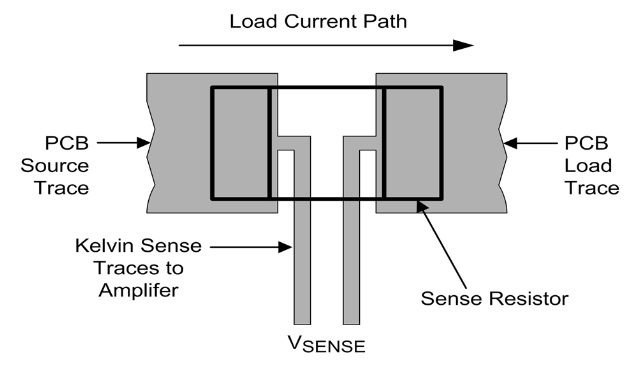
Traces that carry significant current should be wider than signal traces. The table below gives rough guidelines of how wide to make a trace for a given amount of current.
0.010″ 0.3 Amps
0.015″ 0.4 Amps
0.020″ 0.7 Amps
0.025″ 1.0 Amps
0.050″ 2.0 Amps
0.100″ 4.0 Amps
0.150″ 6.0 Amps
When placing a trace, it is very important to think about the space between the trace and any adjacent traces or pads. You want to make sure that there is a minimum gap of 0.007″ between items, 0.010″ is better. Leaving less blank space runs the risk of a short developing in the board manufacturing process. It is also necessary to leave larger gaps when working with high voltage.
When routing traces, it is best to have the snap-to-grid turned on. Setting the snap grid spacing to 0.050″ often works well. Changing to a value of 0.025″ can be helpful when trying to work as densely as possible. Turning off the snap feature may be necessary when connecting to parts that have unusual pin spacing.
It is a common practice to restrict the direction that traces run to horizontal, vertical, or 45-degree angles.
When placing narrow traces, 0.012″ or less, avoid sharp right angle turns. The problem here is that in the board manufacturing process, the outside corner can be etched a little more narrow. The solution is to use two 45 degree bends with a short leg in between.
It is a good idea to place text on the top layer of your board, such as a product or company name. Text on the top layer can be helpful to ensure that there is no confusion as to which layer is which when the board is manufactured.
Checking Your Work
After all the traces are placed, it is best to double check the routing of every signal to verify that nothing is missing or incorrectly wired. Do this by running through your schematic, one wire at a time. Carefully follow the path of each trace on your PC layout to verify that it is the same as on your schematic. After each trace is confirmed, mark that signal on the schematic with a yellow highlighter.
Inspect your layout, both top, and bottom, to ensure that the gap between every item (pad to pad, pad to trace, trace to trace) is 0.007″ or greater. Use the Pad Information tool to determine the diameters of pads that make up a component.
Check for missing vias. ExpressPCB will automatically insert a via when changing layers as a series of traces are placed. Users often forget that via are not automatically inserted otherwise. For example, when beginning a new trace, a via is never inserted. An easy way to check for missing via is to first print the top layer, then print the bottom. Visually inspect each side for traces that don’t connect to anything. When a missing via is found, insert one. Do this by clicking on the Pad in the side toolbar; select a via (0.056″ round via is often a good choice) from the drop-down list box, and click on the layout where the via is missing.
Check for traces that cross each other. This is easily done by inspecting a printout of each layer.
Metal components such as heat sinks, crystals, switches, batteries, and connectors can cause shorts if they are placed over traces on the top layer. Inspect for these shorts by placing all the metal components on a printout of the top layer. Then look for traces that run below the metal components.

trace width calculator to determine how thick and wide your traces should be for your application. Aim for a 5C temperature rise. If you have extra space on the board, use bigger traces, as they don’t cost anything.


درباره این سایت