Practical PCB Layout Tips
Engineers tend to pay most attention to circuits, the latest components, and code as important parts of an electronics project, but sometimes a critical component of electronics, the PCB layout, is neglected. Poor PCB layout can cause function and reliability problems. This article contains practical PCB layout tips that can help your PCB projects work correctly and reliably.
Sizing Traces
Real-world copper traces have resistance. This means that a trace has a voltage drop, power dissipation, and temperature rise when current flows through it. Resistance is defined by this formula:
R=
(resistivity∗length)(thickness∗width)
PCB designers most commonly use length, thickness, and width to control the resistance of a PCB trace. Resistance is a physical property of the metal used to make the trace. PCB designers can't really change the physical properties of copper, so focus on the trace size, which you can control.
PCB trace thickness is measured in ounces of copper. One ounce of copper is the thickness we would measure if we evenly spread 1 oz of copper over a 1 square foot area. This thickness is 1.4 thousandths of an inch. Many PCB designers use 1 oz or 2 oz copper, but many PCB manufacturers can provide 6 oz thickness. Note that fine features like pins that are close together are hard to make in thick copper. Consult your PCB manufacturer about what their capabilities are.
Use a PCB
trace width calculator to determine how thick and wide your traces should be for your application. Aim for a 5C temperature rise. If you have extra space on the board, use bigger traces, as they don’t cost anything.
When doing a multi-layer board, remember that traces on external layers have better cooling than traces on internal layers because the heat from inner layers has to travel through layers of copper and PCB material before being conducted, radiated, or connect away.
Make Loops Small
Loops, especially high-frequency loops, should be made as small as possible. Small loops have lower inductance and resistance. Placing loops over a ground plane further reduces inductance. Having small loops reduces high-frequency voltage spikes caused by
. Small loops also help reduce the number of signals that are inductively coupled into the node from external sources or are broadcast from the node. This is what you want unless you’re designing an antenna. Also, keep loops small for op-amp circuits to prevent noise from being coupled into the circuit.
Decoupling Capacitor Placement
Place decoupling capacitors as near as possible to the power and ground pins of integrated circuits to maximize decoupling efficiency. Placing capacitors farther away introduces stray inductance. Multiple vias from the capacitor's pin to a ground plane reduce inductance.
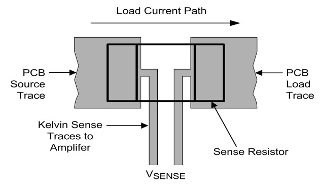
Kelvin Connections
Kelvin connections are useful for measurements. Kelvin connections are made at the exact points to reduce stray resistance and inductance. For example, Kelvin connections for a current sense resistor are placed exactly at the resistor pads, not at some arbitrary place on the traces. Although on the schematic, placing the connections at the resistor pads or at some arbitrary point may look the same, real traces have inductance and resistance that could throw your measurements off if you don’t use Kelvin connections.
Keep Digital and Noisy Traces Away from Analog Traces
Parallel traces or conductors form a capacitor. Placing traces close together capacitively couples the signals on the traces, especially if the signals are high frequency. Keep high frequency and noisy traces away from traces that you don’t want noise on.
The ground is Not Ground!!
The ground is not an ideal conductor. Take care to route noisy grounds away from signals that need to be quiet. Make ground traces large enough to carry the currents that will flow. Placing a ground plane directly under signal traces lowers the impedance of the traces, which is ideal.
در برد مدارچاپی oz به چه معناست؟
HOW SHOULD DESIGN GROUND in ANALOG to DIGITAL BOARD
نکات طراحی PPL ها
طراحی ترک برای برد جریان بالا
همه چیز درباره ی گیرنده ها و ریموت کنترلر های رادیویی ASK


درباره این سایت